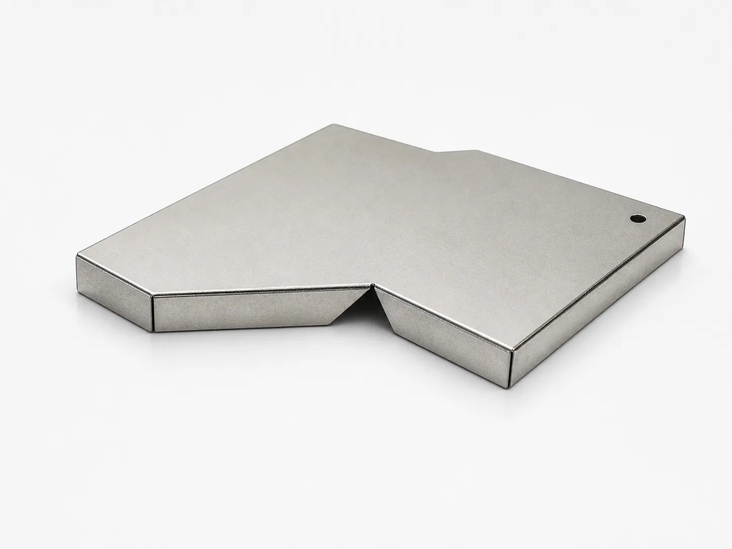
A PCB shielding can is a formed conductive cover placed around selected board-level circuits. It may help control coupling into or out of that area, but the can does not work independently: its seams, openings, PCB landing pattern, grounding path, neighboring components, cables and enclosure all affect the assembled result.
For sourcing, the practical goal is to translate the electrical design into a metal part that can be stamped, finished, assembled, inspected and protected in transit. This guide focuses on those drawing and RFQ decisions. Shielding effectiveness and regulatory compliance remain tied to the buyer's finished assembly and test plan.
Short answer: what defines a quote-ready PCB shield
A quote-ready shield package identifies the protected board area, construction style, controlled 2D drawing, 3D reference, material and thickness, finish, attachment method, PCB landing or mating interface, critical dimensions, burr direction, order quantities, inspection points, packaging and sample plan.
State the buyer's frequency range or EMC concern as context, with the system test method and pass criteria. This explains why seams, tabs or openings are controlled without turning a metal-part quote into an unsupported performance promise.
- Keep the part number, revision and units consistent across drawing, model and RFQ.
- Show nearby component, connector and enclosure clearances that constrain the shield.
- Separate prototype, pilot and annual production quantities.
Choose one-piece or frame-and-lid construction
A fixed one-piece can reduce part count and may suit an area that will not require access after assembly. A two-piece design uses a soldered or otherwise attached frame with a removable lid, making inspection or rework easier but adding a lid-to-frame seam and engagement features that must be controlled.
Construction should follow the assembly sequence. Decide when the shield is installed, whether internal components need visual inspection, and how a technician removes a lid without damaging the board. Request DFM review of draw depth, flange height, corner relief, tabs and lid retention before tooling.
- Fixed can: define attachment tabs and the approved removal method, if removal is ever allowed.
- Frame and lid: define engagement, insertion direction, retention, access and replacement criteria.
Select material and finish for the complete interface
Potential shield materials include tin-plated steel, nickel silver, stainless steel and copper alloys, subject to the supplier's reviewed stock range. Selection involves more than bulk conductivity: formability, spring behavior, corrosion exposure, soldering process, finish availability, cost and interaction with mating materials all matter.
Specify grade, thickness, temper or hardness and surface condition rather than only "metal shield." For plating, identify the finish system, thickness or standard, coverage and masked areas. Tin and nickel finishes may serve different needs, but neither proves a target EMI result. Confirm compatibility with the buyer's soldering, cleaning and storage requirements.
- Identify restricted substances, material certificates and finish reports required for approval.
- Mark areas where finish buildup could change fit or lid engagement.
Design the grounding and PCB landing interface together
The shield needs a defined conductive interface to the board or mating structure. The PCB owner should specify the landing footprint, copper connection, via strategy, solder-mask keepout, pad segmentation and any electrical continuity checks. The metal drawing should reference the same interface through datums, tab locations, flange flatness and contact zones.
A conductive cover cannot compensate for an incomplete return path. Contact can vary with solder coverage, contamination, finish, warpage and assembly force. If a removable lid relies on spring contact, define its engagement and acceptable condition after approved installation or service cycles instead of requiring vague "good grounding."
- Dimension shield tabs or perimeter features to the controlled PCB footprint.
- Mark surfaces that must remain clean, solderable or free of insulating coating.
- Name the buyer-owned continuity or resistance check when one is required.
Control seams, gaps and necessary openings
Every lid joint, corner relief, slot, ventilation pattern and cable clearance changes the conductive boundary. The relevant risk depends on the interference source, frequency range, field orientation, location and return path, so a generic maximum opening rule should not replace EMC review of the actual product.
Ask the electrical team to define maximum opening dimensions and locations, then make them inspectable. Review long slots, removable lid joints and openings close to the circuit of concern. If airflow, tuning or connector clearance requires an aperture, record its function so it is not casually enlarged during DFM.
- Dimension the longest opening span, not only total open area.
- Identify apertures that must align with components, test points or airflow paths.
Make formed geometry, clearance and burr direction inspectable
Thin shielding parts can combine low walls, small tabs, corner notches, embossed areas and close-tolerance openings. Tool access, material thickness, bend relief and springback affect whether those features hold their intended position. Use functional datums and tolerances around the PCB footprint, component height, lid engagement and attachment locations instead of tightening every dimension.
Show the punch-exit burr side or required smooth face. A burr facing the PCB, cable, solder joint or service hand can create risk even when dimensions pass. Define edge-break or deburring needs, recognizing that secondary work can alter small tabs. Include component keepouts beneath the roof and around walls for normal variation.
- Identify maximum formed height, wall position, flatness and coplanarity only where functional.
- Show the PCB side, visible side, smooth side and lid insertion direction.
Plan soldering, installation, rework and packaging
State whether the shield is placed automatically or manually and whether it uses surface-mount tabs, through-board features, clips, screws or another approved attachment. For a soldered design, the PCBA team should confirm pad geometry, paste application, heating profile, cleaning and inspection. The metal supplier needs the resulting dimensions and surface requirements, not responsibility for an undisclosed board process.
Plan orientation and handling. Prevent mirrored installation when geometry is ambiguous, and provide tool access plus controlled instructions for removable lids. Thin shields can nest, tangle, scratch or deform in bulk transport, so specify trays, separators, tubes, tape-and-reel evaluation or another reviewed pack for the assembly line.
- Define pick area, orientation and packaging label requirements when automated placement is planned.
- Approve packaging with production-intent parts before repeat orders.
Separate part inspection from system EMC validation
Supplier inspection can confirm dimensions, material, finish, edge condition, tab position, lid engagement, packaging and other drawing requirements. It cannot establish the final product's radiated or conducted emissions, immunity, radio performance or regulatory compliance from the loose shield alone.
Buyer validation should use the intended PCB, grounding, cables, connectors, enclosure, firmware and operating modes. Compare controlled variants when useful, then run tests selected by the responsible EMC team. Record shield revision, board revision and assembly condition together. Treat changes to openings, contacts, material or attachment as controlled revisions.
- Agree first-article dimensional and appearance records before sample submission.
- Use mating-fit, lid-retention and continuity checks only where the drawing defines them.
Final RFQ checklist for a PCB shielding can
A complete RFQ gives tooling, quality and PCBA teams one controlled definition. Before sending the project, confirm that the quote package distinguishes manufacturing requirements from system targets and identifies who approves each open decision.
- Files: released 2D drawing, STEP/STP model, board-interface reference and revision history.
- Design: one-piece or frame-and-lid construction, material, thickness, finish, datums, tolerances, openings, burr side and keepouts.
- Assembly: attachment method, landing pattern reference, reflow or installation context, rework access, orientation and packaging.
- Commercial: prototype, pilot and annual quantities; tooling ownership; sample count; target schedule; approved alternatives.
- Approval: first-article records, compliance documents, buyer EMC test plan, golden sample and production-release owner.
| Decision | Define on the drawing or RFQ | Buyer review question |
|---|---|---|
| Shielded area | Board footprint, internal keepout, maximum height and nearby interfaces | Which circuit and operating condition drive the EMC concern? |
| Construction | Fixed one-piece, frame and lid, or partitioned layout | Is inspection, tuning or field rework required after installation? |
| Attachment | Solder tabs, through-board features, clips, screws or approved alternative | How does the attachment fit the PCBA assembly sequence? |
| Material | Grade, thickness, temper or hardness and allowed substitutions | Which forming, corrosion, contact and process needs control selection? |
| Surface finish | Finish standard, coverage, thickness, masking and documentation | Is it compatible with soldering, cleaning, storage and mating materials? |
| Ground interface | Landing reference, tabs, contact areas, flatness and no-coating zones | Who owns the PCB copper, vias and electrical continuity criteria? |
| Seams and openings | Lid joint, tab pitch, reliefs, vents and maximum aperture dimensions | Has the responsible EMC engineer approved their size and location? |
| Release controls | First-article checks, packaging, approved sample and change process | Which part checks and system tests are required before production? |